
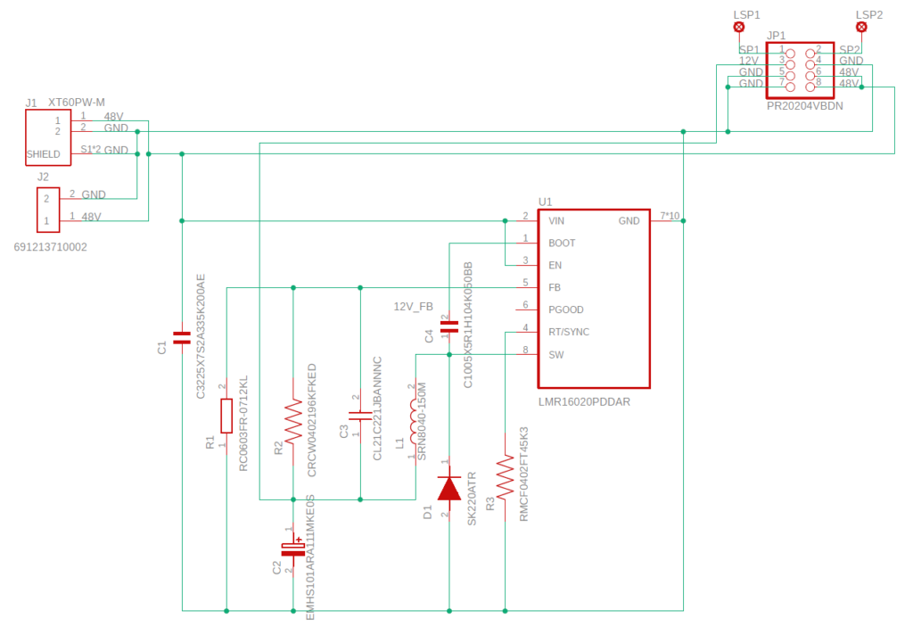
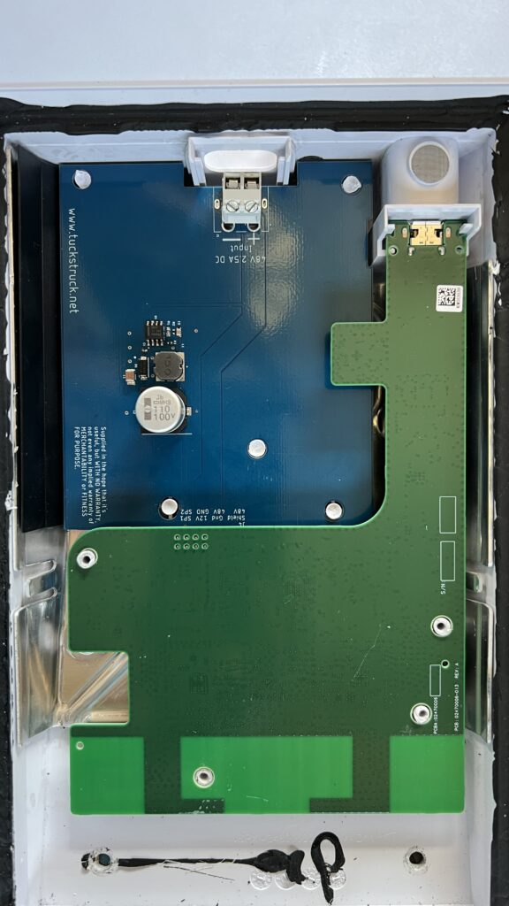
To make converting the rectangular dish Starlink to DC easier I have designed a Starlink 48V PSU adapter PCB to install in place of the original mains power supply. The board is a drop-in replacement that requires a 48V DC supply. The PCB then routes the 48V to the Wi-Fi PCB and creates a 12V supply for the Wi-Fi from the 48V supply. WARNING: 48V DC is a dangerous voltage, do not attempt to use this PCB if you are not sure about what you are doing.
The 12V power supply is designed around a LMR16020 SIMPLE SWITCHER 60 V, 2 A Step-Down Converter. Note the 12V supply output is actually set to 13V as that was the output voltage I measured from the original mains power supply.
Prototype PCB Specification
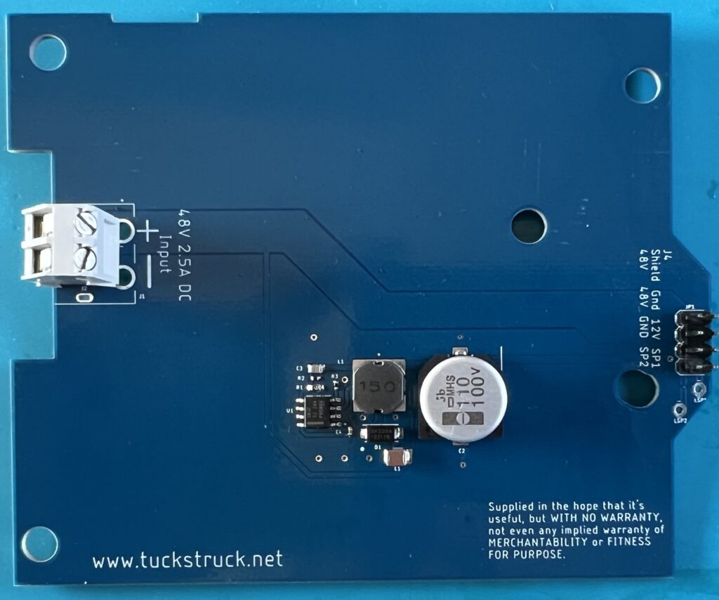
The prototype was built on a 1.6 mm thick FR-4 TG130 PCB with 1oz copper layers and HASL (Hot Air Solder Level) solder pads.
Availability
As we are travelling full time it is impractical for me to start to manufacture these units. However, I am providing all the information you need to make one yourself or have someone else make one for you. I am not going to charge for any of the information. I am not a professional electronics engineer and this is therefore a ‘use at your own risk’ option.
The PCB can be ordered from Seeed Studio here or if you want to order the PCB from another supplier I have uploaded the Gerber files to my Dropbox here.
If you want to use a stencil to assist with applying solder paste, these settings can be used on Seeedstudio for this PCB:
- PCB Dimensions – 10.0cm * 15.0cm Frameless – eff.8*13
- Sides – Top only
- Stencil quantity – 1
- Fiducial Mark – No fiducial
- Thickness – 0.12 mm
- Polishing Technique – Polished
The Zipped Gerber file required for the stencil is the same as the one used for the PCB. You can download this from the gallery page and then load it into the stencil ‘Add Gerber File’ box.
Note: I don’t make money from the PCB sales from Seeedstudio, they’re just the company I used to make the PCB for me. Follow the link above, scroll down to the bottom of the page and you can download the Girber files in a Zip file, which can be used by any PCB company to produce these boards for you.
Here is the Bill Of Materials (BOM) where the components can be ordered:
https://www.digikey.com.mx/en/mylists/list/0L2260K9VS
This is on the Digikey Mexico website but they can supply from Digikey in other countries too (the Mexico website actually ships from the US).
The customer reference in the BOM ties up with the circuit diagram and PCB for the component. This should be printed on the component packets when you receive them to make construction easier.
The PCB has been designed to take an XT-60PW-M plug for the 48V input (J1) instead of a screw terminal (J2) if required (Digikey do not stock them).
Assembly
The PCB is not too complicated but some of the components are very small, 1 mm x 0.5 mm. It could be manually soldered. However, I used a stencil to help apply solder paste to the PCB, also available from Seeed Studio (see link above). The solder paste I used was ‘solder paste no clean 63SN/37PB’: https://www.digikey.com.mx/en/products/detail/chip-quik-inc/SMD291AXT5/8543522?s=N4IgTCBcDaIMoFkAiYCcBGAggDQCoFYBaAOSRAF0BfIA
After applying the solder paste, I positioned all the surface mount components on the board, starting with the smallest.
With all the surface mount components fitted I heated the PCB in a frying pan (a small piece of aluminium foil under the PCB to protect the frying pan). I tried to replicate the heat profile recommended by the solder paste manufacturer by adjusting the heat while monitoring the temperature using an IR temperature sensor. The temperature profile is on a card included with the solder paste or can be seen in the data sheet: http://www.chipquik.com/datasheets/SMD291AXT5.pdf
Once the solder had melted and flowed, I removed the PCB from the frying pan and left it to cool. Once cool I soldered in the 8-pin header connector JP1 and screw terminal J2.
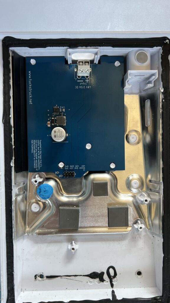
Installation
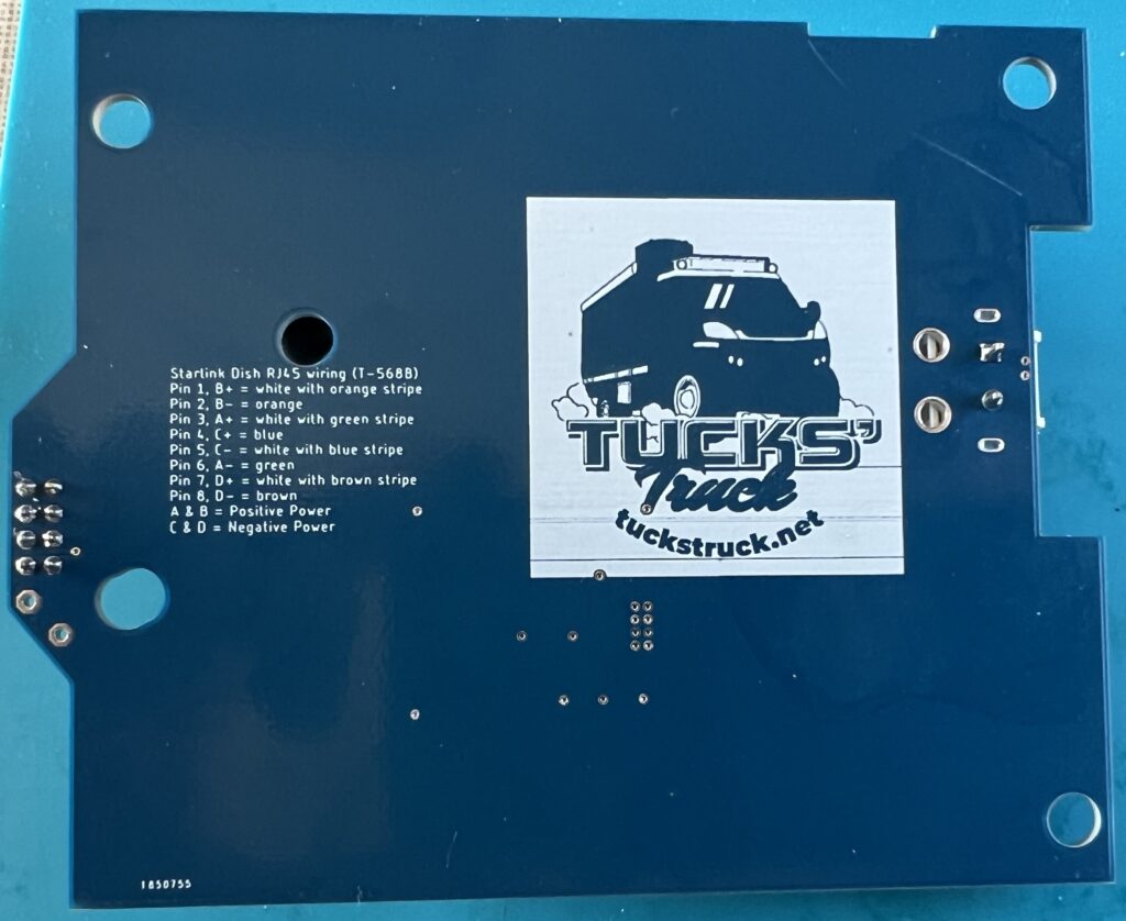
The board is installed in place of the mains power supply PCB. For details about opening the router and removing the PCB see my DC power conversion page here.
You may also be interested in my Starlink Combined DC Power Supply & POE Injector.
If you sign up for Starlink with our referral code (click here), we will each receive one month of free service 30 days after activation. For more information on how it works, check out Starlink support topics here.